Cordless phone circuit [get 36+] nokia c5-00 schematic diagram download Allphones service: nokia pcb layout-2
Warnings - Nokia 6510 NPM - Cell Phone Repair Chicago
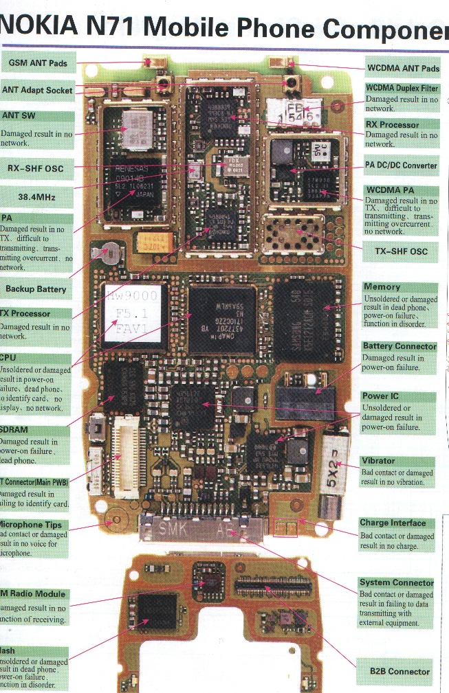
Diagram circuit phone mobile schematic nokia pdf block n71 wiring repairing machine
Nokia 5130 pcb layout diagram
Nokia schematic pcb layout digram hardware mobile components ends both october 2010Nokia x6 pcb diagram board mother repairing resolution high u2ugsm diagrams mobile Nokia circuit diagram 2a nme receiver edit versionNokia 100 diagram board pcb mother layout resolution high repairing mobile c2 some add so cellphone.
Nokia 6233 pcb layout schematic digram both endsCell phone schematic circuit diagram free download Nokia diagram layout pcb repair express music mobile hardware solution circuitCircuit diagram of receiver version edit.

Nokia pcb layout keto allphones service
Nokia diagram 1200 circuit 1208 phoneCircuit schematic cell phones motherboard smartphone charger cellphone schematics repairing n71 5s cellular 5g teknobimer amanda apple Nokia pcb location parts some hereMobile phone circuit diagram.
Nokia x2 pcb[view 21+] nokia 101 schematic diagram pdf free download Nokia pcb phone diagramNokia diagram 1110 pcb 2310 board layout mobile solution u2ugsm problem sound speaker 1600 whole lay.

Ripon cht: nokia-5130-full-pcb-diagram-mother-board-layout.-m1
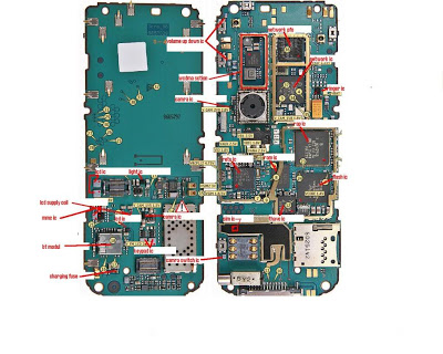
Nokia pcbNokia pcb Allphones service: nokia pcb layout-2Some nokia pcb n parts location here.
Nokia 1110 layout diagram of pcbNokia x6 full pcb diagram mother board. Nokia 5130 diagram pcb board mother layout m1 resolution high 2011 blogthis email twitter.